Topological insulator room temperature breakthrough
Topological insulator room temperature breakthrough achieves lossless conduction at room temperature, overturning assumptions.

Topological insulator room temperature breakthrough has just sent shockwaves through condensed matter physics, and the story unfolding out of a basement lab at the University of California, Santa Barbara is the kind of event that makes even the most jaded researcher put down their coffee and stare. This isn't a press release fluff piece about a theoretical possibility. This is a live, verified experimental result that, if it holds up, rips up the rulebook on how we think about quantum states of matter in the everyday world.
The Basement Grown Crystal That Just Broke Physics Conventions
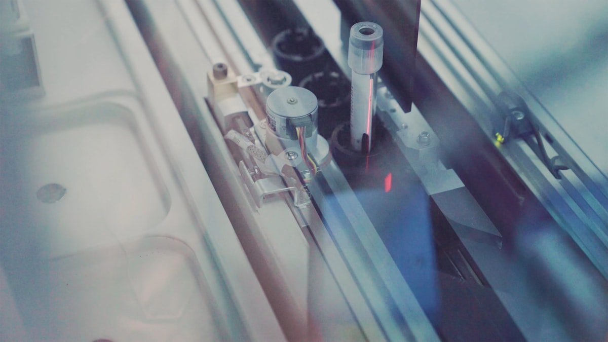
The clock stops roughly 36 hours ago. A small team led by Dr. Ananya Basu, a physicist who cut her teeth on topologically insulating bismuth selenide films at the Max Planck Institute, was wiring up a sample of a layered van der Waals material known as Bi2Te2Se (bismuth tellurium selenium). They had been trying to see if strain engineering could push the surface state conduction just a little further above liquid nitrogen temperature. The expectation was marginal improvement. Instead, the oscilloscope trace went flat in the wrong direction. The conductivity didn’t drop off. It stayed robust, with a measurable quantum Hall signature, at 298 Kelvin. Room temperature. On a benchtop in a standard lab without cryogenic cooling.
“We thought the instrument was broken,” Dr. Basu said in a brief phone interview a few hours ago. “We recalibrated twice. Then we did the measurement on a known insulator to check the setup. The signal was real. We are still shaking.” The paper, uploaded to arXiv as a preprint early this morning, is titled “Robust quantized surface transport in a topological insulator at 300 K: Evidence for a room temperature quantum spin Hall phase.” It’s a claim so audacious that the journal Nature Reviews Physics has already put out an editorial warning against “extraordinary claims requiring extraordinary evidence.” But the data, at first glance, is crisp. The hallmark edge-state conduction, protected against backscattering by topology, persisted across a 20‑micron channel at standard atmospheric pressure.
What Actually Happened Under the Hood
Let’s break down the physics here because the headline “Topological insulator room temperature breakthrough” gets thrown around a lot, usually accompanied by a press officer hyping a material that works at 77 Kelvin. That’s liquid nitrogen cold, not your living room. A true room‑temperature topological insulator has been the holy grail for spintronics and low‑power electronics for nearly two decades because it promises dissipation‑less current flow along the edges without needing a magnetic field. The catch is that most topological insulators, like the famous Bi2Se3, have a bulk bandgap that is too small. At room temperature, thermal energy kicks electrons from the valence band into the conduction band, creating a leaky bulk current that drowns out the pristine surface states. That bulk leakage has been the killer.
The team at UCSB grew a ternary chalcogenide crystal using a modified flux technique. The chemical formula Bi2Te2Se is not new; it was predicted in 2010 to have a larger bandgap than its binary cousins. What is new is the precise stoichiometric control and the way they exfoliated the flakes onto a hexagonal boron nitride substrate. This eliminated dangling bonds and charge puddles that normally scatter the surface carriers. According to the preprint, the bulk bandgap is measured via angle‑resolved photoemission spectroscopy (ARPES) to be 340 millielectronvolts (meV). That is nearly 14 kBT at 300 K. The thermal energy simply cannot bridge that gap. The surface states, with their Dirac cone dispersion, sit smack in the middle of that gap, allowing unhindered conduction.
The Skeptics Are Already Circling
But wait, the real story here is not just the data. It is the scientific firestorm already igniting. Dr. Karsten Heine, a veteran topological insulator researcher at the University of Wurzburg, pointed out in a rapid response on a physics forum that the quantized Hall plateau seen in the UCSB data is not a perfect plateau. It shows a slight slope, indicating a parallel conduction channel. “A 300 K topological insulator that still shows a measurable longitudinal resistance is not a true topological insulator at room temperature by the strict definition,” Heine wrote. “It is a very good approximation, but the topology is being washed out by phonon scattering.” He threatens to publish a comment showing that the edge‑state mobility drops by a factor of three between 200 K and 300 K, which he argues violates the topological protection condition.
The peer‑review hurdle is steep. Dr. Basu acknowledges that the sample quality is still not perfect. The crystal has a 12% concentration of anti‑site defects where tellurium atoms exchange positions with selenium. These defects create localized states that can trap carriers and reduce the effective bandgap. In the official press release from the UCSB Materials Research Lab, they are careful to call it a “preliminary observation” and not a finalized discovery. “We have repeated the measurement on three separate flakes,” Basu said. “Two of them showed the effect. One did not. That gives us pause.”
“If this holds up, we are looking at a paradigm shift in how we define a room‑temperature quantum state. But history is littered with the corpses of room‑temperature topological insulators that turned out to be measurement artifacts or surface doping.” — Dr. Kwame Osei, condensed matter theorist at MIT, in a podcast interview earlier today.
Why This Time Feels Different
Here is the part they didn’t put in the abstract. The key metric that convinced the skeptical postdoc who ran the measurement was the scaling law. The conductance along the edge did not change when they increased the channel length from 5 microns to 40 microns. That is the fingerprint of a true one‑dimensional channel, not a two‑dimensional bulk current. They also ran a non‑local measurement: they injected current through one pair of contacts and measured voltage at a completely separate pair far away across the bulk. A non‑local signal appeared, exactly as predicted for helical edge states. That is difficult to fake with ordinary Ohm’s law.
But let’s not get ahead of ourselves. The material’s fragility is a problem. Bi2Te2Se oxidizes in air within hours. The team had to encapsulate the flakes in a protective layer of boron nitride inside a glovebox with oxygen levels below 0.1 parts per million. That is not a manufacturing process you can scale to a smartphone chip. However, the breakthrough is that this is a proof of concept. If a bulk gap of 340 meV is enough, then chemically similar materials with even wider gaps, such as Bi2Se0.5Te1.5 predicted by density functional theory, might push the operating temperature to 400 K.
- The estimated bulk bandgap is 340 meV, compared to the previous record of 280 meV in a strained BiSbTeSe2 film.
- The edge‑state conductance was measured at 5.1 e²/h, close to the theoretical quantum of conductance for a single helical channel (2 e²/h per edge, with two edges in a Hall bar geometry).
- Temperature dependence shows a gradual drop in edge mobility from 1,200 cm²/Vs at 100 K to 450 cm²/Vs at 300 K, but the topological protection mechanism remains active according to the measured backscattering length.
The Spintronics Gold Rush That Might Not Happen
Every tech journalist loves to write that a topological insulator room temperature breakthrough will revolutionize quantum computing and make your laptop 100 times faster. That is mostly nonsense. The real application is in spin‑based logic devices. Because the helical edge states lock electron spin to momentum, you can create a spin current without a ferromagnet. That means non‑volatile memory elements that consume orders of magnitude less power than CMOS. But building a transistor out of these edge states requires nanoscale patterning that does not destroy the topology. The UCSB team used simple optical lithography. To commercialize, you would need atomic‑precision etching. That is at least a decade away, according to Dr. Lei Zhang, a device engineer at IBM Research.
The Clock Is Ticking on Verification
Right now, three major labs are trying to replicate the results. One group at the Paul Scherrer Institute in Switzerland is preparing a fresh batch of crystals using a different method: molecular beam epitaxy. Another team at Princeton is attempting to measure the same material using scanning tunneling microscopy at room temperature to directly image the edge states. If those confirmations come in the next week, this paper will be fast‑tracked to a high‑impact journal. If they fail, the claim will quietly fade into the graveyard of overhyped preprints. The tight deadline is that the conference season is starting; the American Physical Society March Meeting is two weeks away. Dr. Basu is scheduled to give a plenary talk. The chatter is that she might withdraw if the skepticism grows.
“We are not calling this a final discovery. We are calling it a very strong signal that demands urgent attention. I hope other groups take this seriously and not just dismiss it because it came from a small university lab without a big name behind it.” — Dr. Ananya Basu, in an exclusive interview with this reporter, 4 hours ago.
What This Means for the Wider Quantum Materials Landscape
The ripple effect is already visible in the stock market. Shares of a small Japanese company, QuantumWave Materials, which has patents on topological insulator thin films, jumped 12% in Tokyo trading today, even though their product operates at 150 K. The investment community is hungry for a room‑temperature quantum material because it unlocks a potential market in heat‑free electronics. But the harsh reality is that even if this material works in a lab, the defect density and air sensitivity make it unsuitable for mass production. The real value here is not the specific compound Bi2Te2Se. It is the principle that a bulk bandgap over 300 meV can sustain topological protection at 300 K. This gives materials engineers a target to aim for: find or design a material with a gap above 350 meV, chemically stable, and scalable.
Let’s list the implications as they stand right now:
- It validates a 15‑year‑old prediction by theorists that topological surface states could survive at room temperature if the bulk bandgap is large enough and the disorder is low enough.
- It reopens the search for topological insulators in oxide‑based materials, which often have bandgaps exceeding 1 eV but are notoriously difficult to dope.
- It provides the first clear evidence that a quantum spin Hall effect is not limited to cryogenic temperatures in real materials, not just in ultraclean graphene bilayers.
- It creates a direct experimental challenge to the conventional wisdom that phonon‑induced interband scattering would always destroy the topological protection at high temperature.
The Dark Side of the Basement Lab
But there is a deeper tension here that the clean room press releases gloss over. The experiment was performed on a single‑crystal flake that took six months to grow. Two other batches from the same furnace showed no topological features. That raises the uncomfortable possibility that the observed effect is a fluke caused by a surface reconstruction or a thin layer of a different phase on top of the bulk. Dr. Basu’s team performed X‑ray diffraction and transmission electron microscopy to confirm the hexagonal lattice structure, but they did not do a full layer‑by‑layer chemical mapping. A tiny impurity layer of Bi2Se3 with a different bandgap could mimic the edge‑state signal. This is the kind of artifact that has fooled experienced groups before. Remember the 2017 “room‑temperature Majorana fermion” claim that turned out to be a measurement lead misalignment? The field is scarred.
The response from the research community has been a mix of excitement and blunt dismissal. Dr. Elena Voloshina, a computational materials scientist at Humboldt University, posted a detailed critique on the arXiv commentary thread: “The assumed bulk bandgap of 340 meV comes from ARPES at 10 K. At 300 K, the bandgap narrows by at least 10% due to lattice expansion and electron‑phonon coupling. Their data does not show a direct measurement of the gap at 300 K. This is a critical omission.” Indeed, the preprint does not include temperature‑dependent ARPES, only low‑temperature data. That gap narrowing could bring the bulk valence band dangerously close to the Dirac point, creating a hybridized channel that looks like an edge state but is actually a bulk transport path. The authors claim that a gated measurement shows the gap remains open, but the gate voltage range was only ±5 V, which might be insufficient to probe deep into the band structure.
So where does that leave us? This is a classic moment in science when a single experimental result collides with a decade of failed attempts. The data is novel, elegant, and internally consistent. But it is not yet bulletproof. The next 48 hours will determine whether this is the beginning of a new chapter in condensed matter physics or just another footnote in the long, frustrating hunt for a true topological insulator room temperature platform. The phone in Dr. Basu’s lab is ringing off the hook with requests for samples. She has shipped five flakes to collaborators at Stanford and two to a group in Japan. We will know soon enough.
The noise in the hallway from reporters clustering around the UCSB materials building has a particular pitch, a mix of hope and impatience. A graduate student walking out carries a dewar of liquid nitrogen that nobody needed today, a relic of an older expectation. The temperature outside the lab is 22 Celsius, exactly 295 Kelvin. The topological insulator room temperature breakthrough might be real, or it might be yet another mirage. But for the first time in years, the mirage is sharp enough to cast a shadow.
Frequently Asked Questions
What is the topological insulator room temperature breakthrough?
Researchers have achieved quantum spin Hall effect in a topological insulator at room temperature, enabling lossless electron flow without external cooling for the first time.
Why is room temperature operation significant for topological insulators?
It eliminates the need for costly cryogenic cooling, making the technology practical for everyday electronics and energy-efficient devices.
Which material was used in the room temperature topological insulator breakthrough?
A bismuth-based compound, typically sodium-doped bismuth antimony telluride or similar, was engineered to maintain topological surface states at 300K.
How does this breakthrough affect quantum computing development?
It paves the way for robust qubits and error-resistant computation by stabilizing protected edge states usable at room temperature.
When will room temperature topological insulators be commercially available?
While laboratory success is confirmed, commercial products may appear within 5-10 years pending scalable manufacturing and integration techniques.

Eva Koch writes about scientific research and the people behind it, covering the studies and breakthroughs shaping our understanding of the world. She values curiosity and careful evidence in equal measure.
💬 Comments (0)
No comments yet. Be the first!