Applied Materials AI Lab Aims to Halve Chip Dev Time
Applied Materials AI lab, a new $5 billion EPIC facility, aims to halve chip development time, fostering collaboration with industry partners.
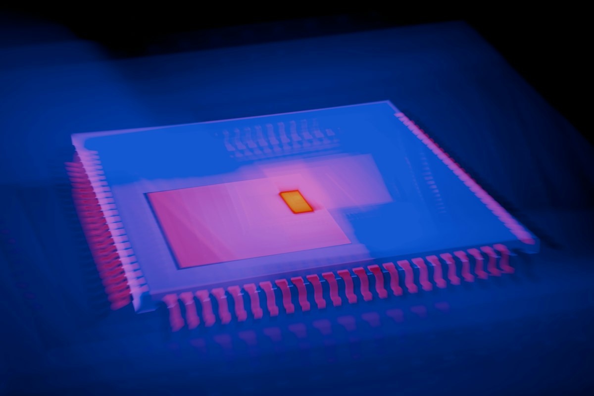
Applied Materials AI lab, a monumental $5 billion research and development center, has officially opened its doors in Sunnyvale, California. This expansive facility, named EPIC, signals a determined effort to drastically accelerate chip development, with the ambitious goal of cutting the typical "concept to commercialization" timeline for new chip architectures by half, from 10-12 years to as little as six. The unveiling of this 600,000-square-foot structure marks the largest-ever U.S. investment in advanced semiconductor equipment R&D, a clear statement in the intensifying global race for technological supremacy.
A New Nexus for Chip Innovation
The EPIC center, a two-year construction project situated on Applied Materials’ campus near its headquarters, stands as a striking symbol of ambition in a region often criticized for lacking substantial manufacturing infrastructure. Built with materials equivalent to two Eiffel Towers' worth of steel, its imposing presence contrasts sharply with the area's generally unassuming corporate buildings. This facility is not merely a showcase; it is a collaborative hub designed to unite leading industry players under one roof.
Chip titans are partnering. They're committing their own teams of researchers to work directly on-site. And these collaborations are expected to generate unprecedented breakthroughs by giving partners early access to Applied Materials' latest equipment and expertise.
- Intel
- TSMC
- Micron
- SK Hynix
- Samsung
Within the facility, "clean rooms" spanning the size of three football fields will host researchers in specialized suits, operating advanced machinery to etch microscopic circuits onto silicon wafers. This is vital work. Competing companies will be there. You'll find Micron and SK Hynix. They're memory chip manufacturers. So, they'll operate their own private test facilities. These come replete with sophisticated chipmaking gear, and they'll collaborate closely with dedicated teams from Applied Materials.
Streamlining the Path to Breakthroughs
The core philosophy behind the EPIC center centers on accelerating the notoriously lengthy process of bringing new chip generations to market. By co-locating innovators and providing earlier access to foundational technologies, the initiative aims to increase the likelihood of successful breakthroughs while minimizing costly dead ends in research.
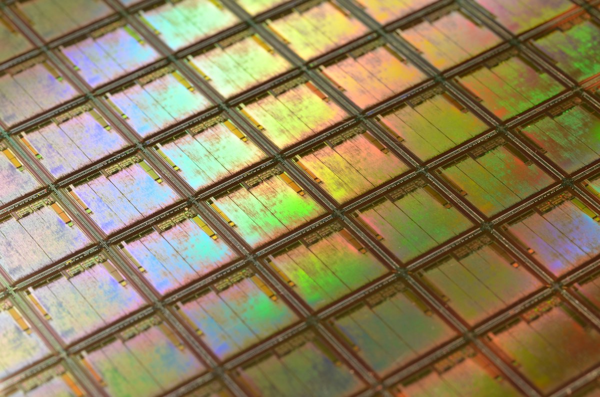
“Having innovators co-located together, having earlier access to the technologies that enable new AI architectures, profoundly alters the industry dynamics,” stated Gary Dickerson, CEO of Applied Materials, during an interview at the event. He emphasized that without such direct collaboration, companies often remain unaware of critical technical possibilities.
This integrated approach promises to provide a more thorough understanding of technical feasibility at earlier stages of development. The goal is clear: shave years off the development cycle, pushing innovation forward at an unprecedented pace to meet the insatiable demands of artificial intelligence.
Silicon Valley's Enduring Edge
While the EPIC center is dedicated purely to research and not commercial production, its role in maintaining Silicon Valley and Applied Materials at the forefront of advanced chip technologies is undeniable. This investment is a vital strategic asset in the global competition to develop more powerful AI models. The urgency of this mission was underscored by recent news: CXMT, a memory manufacturer in China, announced a potential breakthrough in memory chip density. Such an advancement, if verified, could enable CXMT to produce more power-efficient memory chips, potentially surpassing Samsung and SK Hynix.
The U.S. government has actively restricted the sale of advanced GPU chips and specific chipmaking equipment to China, a measure intended to limit the computing power available for developing advanced AI models that could rival those from U.S. companies like OpenAI, Anthropic, and Google. Dickerson frequently referenced "winning the AI race" at the event, though he refrained from commenting directly on U.S. export regulations concerning China. Applied Materials itself previously paid $252 million to settle a case with the U.S. Department of Commerce regarding allegations of shipping equipment to China in violation of export restrictions.
Market Dynamics and Future Demand
Founded in 1967 as a chemistry supply company serving the nascent semiconductor industry, Applied Materials has evolved into the world's leading provider of chip manufacturing equipment. The company has seen major gains from the recent AI boom and the subsequent scarcity of memory chips; its shares have climbed over 110% in the past year. In August, the company reported strong quarterly revenue of $9.12 billion, marking a 25% increase year-over-year. Management has also indicated strong visibility into customer demand extending as far as 2030.
The outlook seems positive. But some observers caution. They cite the memory chip industry's historical boom and bust cycles. Overinvestment by both chipmakers and equipment providers could pose real risks. Demand might soften. And visibility into future demand, while it's helpful for planning, doesn't equate to firm, signed contracts, they warn.
Confidence Amidst Rapid Change
Dickerson, however, remains confident in the sustained demand for chips, driven by the proliferation of new products and services leveraging AI. He anticipates an ongoing need for advancements in both performance and power efficiency.
The pace of innovation is accelerating dramatically. “This is moving so quick,” he remarked. “There’s never been an inflection like this in our lifetimes.” This sentiment encapsulates the urgency and strategic importance of facilities like the Applied Materials AI lab in shaping the future of technology.
```Frequently Asked Questions
What is the Applied Materials AI lab, and what is its primary objective?
The Applied Materials AI lab, also known as EPIC, is a monumental $5 billion research and development center located in Sunnyvale, California. Its primary objective is to drastically accelerate chip development, with the ambitious goal of cutting the typical 'concept to commercialization' timeline for new chip architectures by half, from 10-12 years to as little as six.
Who are some of the key industry players collaborating at the EPIC center?
Leading industry players such as Intel, TSMC, Micron, SK Hynix, and Samsung are partnering and collaborating at the EPIC center. These companies commit their own teams of researchers to work directly on-site, with some like Micron and SK Hynix operating their own private test facilities within the center.
How does the EPIC center aim to streamline the path to breakthroughs in chip development?
The EPIC center aims to streamline breakthroughs by serving as a collaborative hub where innovators are co-located under one roof, providing earlier access to foundational technologies. This integrated approach is expected to increase the likelihood of successful breakthroughs while minimizing costly dead ends in research by providing a more thorough understanding of technical feasibility at earlier stages.
What is the significance of the Applied Materials AI lab's investment in the context of the global semiconductor industry?
The Applied Materials AI lab represents the largest-ever U.S. investment in advanced semiconductor equipment R&D, valued at $5 billion. This investment is a vital strategic asset in the global competition to develop more powerful AI models and maintain Silicon Valley and Applied Materials at the forefront of advanced chip technologies.
What kind of work specifically takes place within the clean rooms of the EPIC center?
Within the EPIC center's clean rooms, which span the size of three football fields, researchers operate advanced machinery. Their work involves etching microscopic circuits onto silicon wafers to develop new chip architectures. Partner companies also conduct specialized research and testing in their dedicated facilities.

Julian Sterling reports on enterprise IT, data infrastructure and the vendors that keep modern business running. He has a long-standing interest in how organisations modernise their systems without breaking what already works.
💬 Comments (0)
No comments yet. Be the first!